
Intel's XBM Patent Rethinks AI Memory
Intel wants to ditch HBM's costly silicon interposer with a chiplet-native memory stack, but it's still just a patent.
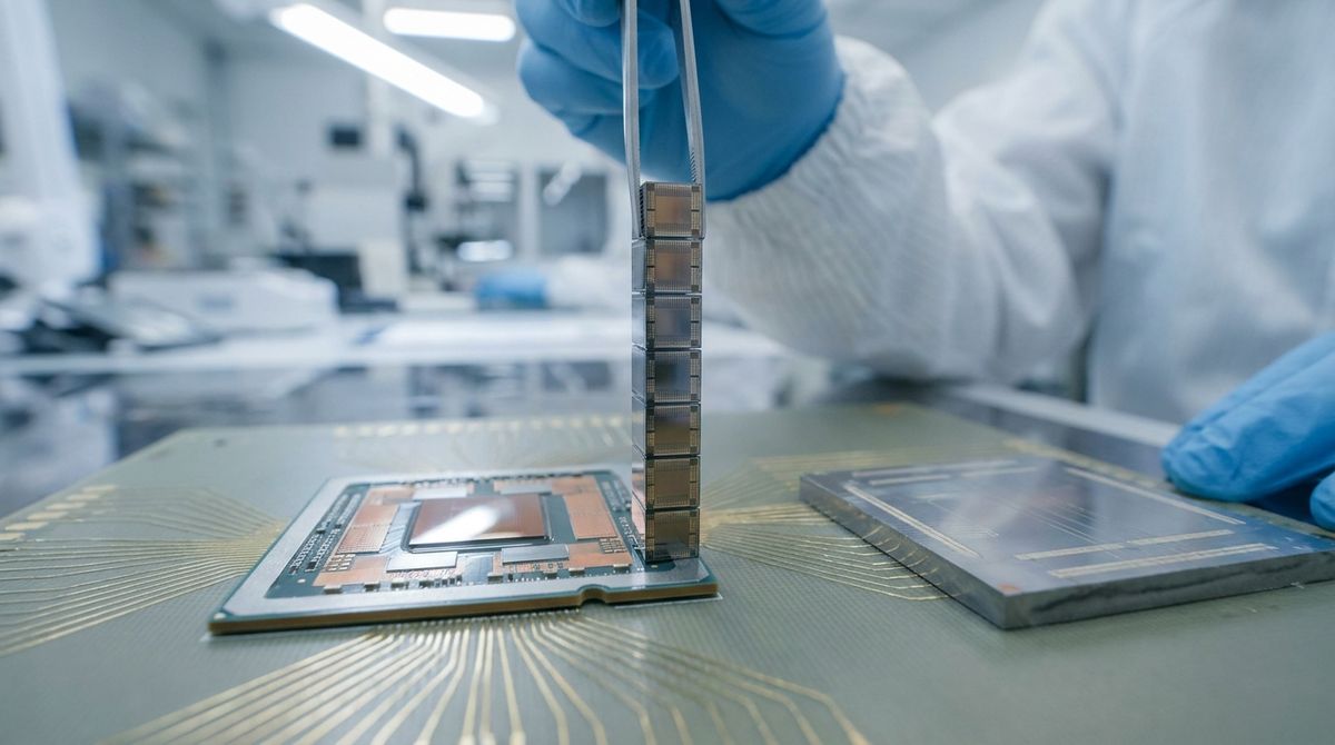
AI chips have a feeding problem. The processors that run large models have gotten so fast that memory can't shovel data at them quickly enough, a chokepoint engineers politely call the "memory wall." That is why the current darling of AI hardware, high-bandwidth memory (HBM), is both essential and infuriatingly expensive to build.
A newly published Intel patent application, spotted by the account Underfox, hints at how Intel might sidestep some of that cost. It describes an architecture called cross-batch memory, or XBM, and it takes aim squarely at the parts of HBM that make it pricey and hard to scale.
What HBM does today
Standard HBM stacks memory chips vertically, threads them together with tiny vertical wires called through-silicon vias, and talks to the processor across a silicon interposer. That interposer is a slab of silicon that acts as a fancy circuit board, carrying an extremely wide connection of around 1,024 wires per stack. All that width is how HBM moves so much data. It is also what makes packaging it a costly, finicky affair, since every one of those wires has to be routed just so.
What Intel is changing
XBM makes two big moves. First, it changes where the memory lives. Normal DRAM cells sit in the base silicon layer where transistors are usually built. Intel instead builds the memory cell higher up, in the metal-and-wiring layers above the transistors, using thin-film transistors. That approach, called back-end-of-line fabrication, lets Intel chop each die into many small, independently addressable blocks. The filing describes dies of roughly 1.5 gigabytes each, stacked eight high and scaling to sixteen.
Second, and more consequentially, it drops HBM's wide parallel connection. Instead of a thousand-plus wires crossing an interposer, XBM funnels data out over UCIe links running at 32 gigatransfers per second. UCIe (Universal Chiplet Interconnect Express) is an industry-standard way for chip building blocks to talk to each other, and using it makes the design "chiplet-native." Intel's argument is that a standard serial interconnect is simpler and cheaper to package than an interposer-bound stack.
There is a catch worth flagging: 32 gigatransfers per second is UCIe's current top speed. In other words, XBM would launch already pressed against the spec ceiling, with no obvious room to go faster.
Fixing defects after the fact
Tall memory stacks are hard to build without flaws, and a single bad cell can sink an otherwise good chip. Intel leans hard on repairability here. The base die at the bottom of the stack carries spare channels, built-in self-repair logic, and redundant memory arrays that can stand in for defects in the dies above. The idea is to claw back manufacturing yield after assembly rather than throwing away expensive stacks.
A surprising chunk of the filing is not about the memory at all, but about how to mount it. Intel details packaging tricks to shrink the stack's height and remove a stiffening component normally needed to stop the package from warping. That is the concrete basis for its "smaller, cheaper package" pitch.
One of two bets
XBM should not be confused with ZAM, a separate memory architecture Intel is co-developing with SoftBank subsidiary SAIMEMORY and plans to present at the VLSI Symposium 2026, with commercialization aimed at 2029. ZAM keeps largely conventional DRAM but innovates on how the layers are bonded together. Read side by side, the two suggest Intel is hedging with at least two HBM alternatives. Fitting, perhaps, for a company that started life as a memory maker back in 1968.
What's next
Temper the excitement. This is a patent application filed in December 2024, not a product or even a roadmap. It signals intent, not a shipping part. Backend-transistor DRAM remains unproven at manufacturing scale, the UCIe interface is already maxed out, and XBM would still have to prove itself against newer HBM generations and Intel's own ZAM timeline. Patents are cheap; competitive memory is not. Still, the fact that so many players are attacking the interface rather than the logic tells you where the real bottleneck now sits.